SEMICONDUCTORS
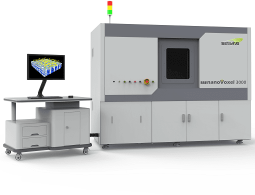
NanoVoxel-3000
equipped with a transmissive open-tube X-ray source system with high resolution, which is suitable for high-resolution inspections, especially for low- and medium-density samples.
BENEFITS
- Open tube transmission (microfocal/nanofocal).
- Voltage up to 240KV / 225KV / 190KV / 160KV
- Non-destructive testing
- Sub-micron resolution for detection of defects
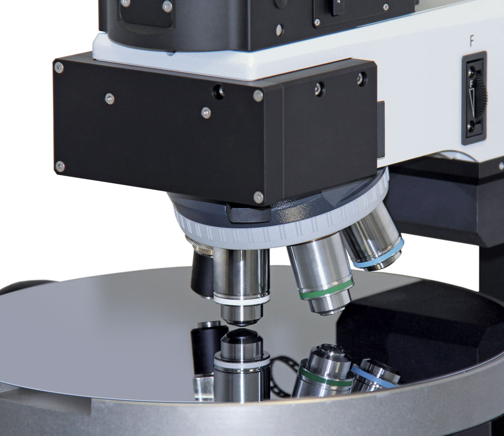
alpha300R Semiconductor Edition
a high-end confocal Raman and photoluminescence (PL) microscope specifically configured for the chemical imaging of semiconducting materials.
BENEFITS
- Full inspection of up to 12 inch wafers
- Able to investigate inherent strain and crystalline properties of device structures.
- Can be combined with other techniques such as AFM, SEM, SNOM
- Optimized spectrometer for high resolution imaging and fast speed mapping